Guide – How to: design a single-core SoC
This guide illustrates how to generate and test a minimal single-core ESP SoC. In doing so, this tutorial covers the basics of SoC configuration, full-system RTL simulation and FPGA prototyping with the ESP platform.
Note: The users have access to prebuilt material to run the tutorial on an FPGA, without executing all the previous steps. See the ‘FPGA prototyping with prebuilt material’ section at the end of this guide.
Target FPGA board
ESP currently supports multiple FPGA boards as listed in the homepage. The
socs/ directory of ESP contains a design folder for each of the target
FPGA boards. The steps described in this guide are identical for all the FPGA
targets, but they should be run from the design folder in socs/
corresponding to the desired target.
For this tutorial we target the popular Xilinx VC707 evaluation board based on the Virtex7 FPGA.
# Move to the Xilinx VC707 design folder
cd <esp>/socs/xilinx-vc707-xc7vx485t
Running `make help` in the design folder prints a description of the most common *Make* targets in ESP, many of which are described in this tutorial.
SoC configuration
Each design folder comes with a default SoC configuration
(socs/defconfig/esp_<design-folder-name>_defconfig), which consists of a 2x2
mesh with one processor tile, one memory tile containing a memory controller and
one auxiliary tile. This is the minimum set of tiles for a functioning ESP
SoC. Depending on the design folder the default configuration may differ in the
processor core selection (e.g. RISC-V Ariane or SparcV8 Leon3) and in the
presence of the ESP cache hierarchy.
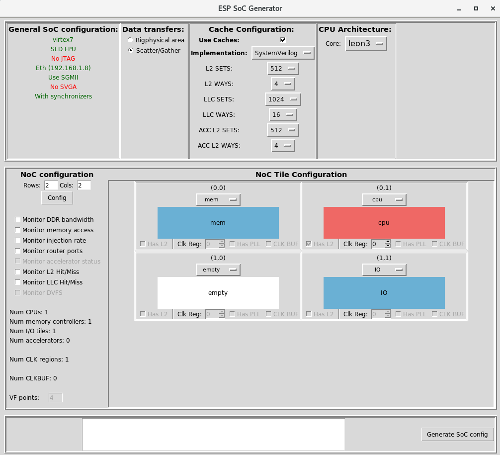
The SoC configuration can be visualized and modified with the ESP configuration GUI:
make esp-xconfig
The figure below shows the GUI with the default configuration for the
Xilinx VC707 board. In this case the selected CPU is the Leon3 processor and
the ESP caches are enabled: one 32KB 4-ways set associative private L2 cache for
the processor tile and one 256KB 16-ways set associative last-level cache (LLC)
on the memory tile. In this design the LLC serves only the processor tile and
the Ethernet MAC in the miscellaneous (IO) tile.
 {:height=”812px” width=”684px” align=”center”}
Note: The ESP caches do not work with the Ariane core yet. This feature is in the works.
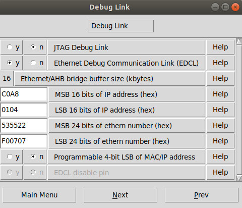
Debug link configuration
The ESP SoC embeds some IP blocks from the open source VHDL library GRLIB,
including the Leon3 processor core and some I/O peripherals. The default
configuration for GRLIB is loaded from the file
socs/defconfig/grlib_<design-folder-name>_defconfig. The GRLIB
configuration utility starts with the following command:
make grlib-xconfig

One relevant configuration parameter is the static IP assigned to the Ethernet debug interface. A host machine can control the debug interface of an ESP SoC through Ethernet only. By clicking on Debug link on the GRLIB GUI it is possible to configure the static IP of the debug unit by editing the two IP address fields.
Given an ESP SoC on FPGA there are two possible ways to access it through
Ethernet from a host machine: with a direct link or through a router. In the
following, as an example, we assume you selected the IP address of the debug
link to 192.168.1.2 (MSB = C0A8 and LSB = 0102).
a) Direct link
Connect with an Ethernet cable the Ethernet ports of FPGA and of the host
computer that you wish to interact with the ESP SoC on FPGA. From your system
settings, turn off the wired internet connection. Then, from a terminal, assign
a valid IP address to your interface using the same three numbers of the ESP
debug link (192.168.1 in this example) and varying the last one. This
guarantees that your host machine will be in the same subnet as the ESP debug
link, so that it will be possible to establish a connection between the two.
In this example we assume your Ethernet interface name is eth0. (You can find
out the specific name of the interface by typing ifconfig in your shell.)
# assign an IP address to your host machine
sudo ifconfig eth0 192.168.1.3
b) Link through a router
With two Ethernet cables, connect the Ethernet ports of both your FPGA board and
your host computer to a router. The IP address assigned to the ESP debug link
must be in the subnet selected by the router. For instance, if the router
assigns IP addresses in the range 192.168.1.2 to 192.168.1.255, then any IP
address in that range can be used for the ESP debug link. From the admin webpage
of the router you should be able to change the range of assigned addresses, as
well as to reserve a specific IP to the MAC address corresponding to the ESP
debug link. Reserving the IP will guarantee that no other device connected to
the router will get the IP of the debug link through a DHCP request.
In case your host computer received the same IP you selected for the debug link, you can force a new lease with the following:
# assign an IP address to your host machine
sudo ifconfig eth0 192.168.1.3
It is, however, recommended to reserve the IPs from the router's admin page rather than forcing the IP assignment from the host computer.
ESP Cache Hierarchy
With a single-core SoC, you have the option of using ESP’s cache hierarchy,
which adds a private L2 cache to CPUs (and optionally, to accelerators) and
a last-level cache to the memory tile (the LLC is partitioned if multiple
memory tiles are selected). The checkbox labeled Use Caches enables the
cache hierarchy, which is the default setting. There are two options for the
implementation of the caches – SystemVerilog and SystemC + HLS – which can
be selected from the dropdown menu labeled Implementation in the ESP
configuration GUI. The SystemVerilog caches offer area savings and slight timing
improvements and is the default. Note that with the SystemVerilog implementation
, the CPU L2 and accelerator L2 caches must be configured to have the same
number of sets and ways. For more information on the HLS-based cache hierarchy,
read the section below.
Optional: HLS-Based Cache Hierarchy
As shown above, the default SoC for the Xilinx VC707 board has the ESP cache
hierarchy enabled. By default, the RTL implementation is selected. If you want
to switch to the SystemC version, select SystemC + HLS from the
Implementation dropdown in the ESP configuration GUI. This feature is
particularly useful to conduct architectural research on coherence, because the
SystemC model is significantly easier to edit than the RTL implementation.
To generate the RTL for the SystemC version of the caches, a one-time HLS run is required for every desired combination of sets and ways of the caches.
make l2-hls
make llc-hls
These commands run HLS with Cadence Stratus HLS for all the combinations
of {sets, ways, words per line, word bitwidth, address bitwidth} specified in
HLS TCL scripts: systemc/l2/stratus/project.tcl,
systemc/llc/stratus/project.tcl. The first HLS run takes a long time, because
it synthesizes hardware resources from scratch, whereas the subsequent HLS runs
are much faster.
The ESP cache hierarchy is mandatory only for multi-core ESP SoCs. If the caches are not enabled in the ESP configuration GUI, or if using the RTL implementation, this step can be skipped.
Note: A Verilog implementation of the HLS-based cache hierarchy will be released soon (pending approval).
RTL simulation
Users can run a full-system RTL simulation with the following targets:
# Modelsim
make sim[-gui]

# Incisive
make ncsim[-gui]
Once Modelsim starts you can launch with the simulation with the command:
make run --all
These simulation targets compile the RTL from ESP and from some Xilinx
libraries. In addition to RTL files, the simulation targets cross-compile the
default C application systest.c for the target processor. Then the simulator
starts either in the terminal (e.g. make sim) or with the GUI (e.g. make sim-gui).
Users can edit systest.c at will, as long as the baremetal cross-compiler can
generate the target binary. The output of this compilation are the memory files
for simulation (prom.srec and ram.srec) and the target binaries for FPGA
emulation of the baremetal test (prom.bin and systest.bin).
Users can run the software compilation step independently from the simulation target with:
make soft
[Back to top](#)
FPGA prototyping
Bitstream
The deployment of an ESP SoC on FPGA requires a FPGA bitstream, whereas its testing requires the binary of a baremetal application and/or a Linux image.
Below is the target to generate the FPGA bitstream with Xilinx Vivado from the
design folder based on what specified in the GRLIB and ESP configurations. After
Vivado completes the bitstream generation, a link to the bitstream top.bit
is created in the SoC design folder.
# Logic synthesis for FPGA with Xilinx Vivado
make vivado-syn
Bare-metal and Linux applications
The binary of the baremetal application (prom.bin and systest.bin) is
compiled with make soft as described in the previous section.
Linux is also compiled from the ESP SoC folder. This allows users to maintain
different Linux configurations and root filesystem overlays for each SoC
folder. The following command configures and compiles Linux with the root
filesystem template created with the scripts to build the toolchain. Users can
add, edit or remove files from the local copy of the filesystem placed in
sysroot/. Re-running the Linux target below will update the embedded root file
system. The final output of this target is a bootable Linux image (linux.bin).
make linux
FPGA programming
Assuming the FPGA host computer is localhost and the TCP port is the default
3121, the ESP instance can be deployed on FPGA with the following command:
# Program FPGA
FPGA_HOST=localhost XIL_HW_SERVER_PORT=3121 make fpga-program
If you are using a remote FPGA device and the JTAG cable is connected to a remote host computer, set `FPGA_HOST` and `XIL_HW_SERVER_PORT` to the appropriate values. The remote server must be running an instance of *Vivado hw_server*.
UART interface
After programming the FPGA, the ESP UART interface must be opened with a serial
communication program (e.g. minicom) to monitor the programs executing on the
ESP instance.
With the USB cable provided by the FPGA board vendor, connect the UART port
to any USB port on your computer. Then run dmesg to find the device name assigned
to the new serial interface. Here is an example:
$ dmesg | grep tty
[352854.825049] usb 1-2: cp210x converter now attached to ttyUSB0
For instance, if your serial interface has been labeled ttyUSB0, you may
connect to /dev/ttyUSB0 with your favorite serial communication program. In
this example we will refer to Minicom. The serial interface should be
configured to use no parity bits, no flow control and a baud rate of 38400. To
configure Minicom launch it with sudo minicom -s.
 +-----------------------------------------+
 |     Serial Device      : /dev/ttyUSB0   |
 |  Lockfile Location     : /var/lock      |
 |    Callin Program      :                |
 |   Callout Program      :                |
 |     Bps/Par/Bits       : 38400 8N1      |
 |  Hardware Flow Control : No             |
 |  Software Flow Control : No             |
 +-----------------------------------------+
Now you can launch Minicom:
minicom -D /dev/ttyUSB0 -b 38400
Please note that standard users on Linux do not have permission to connect to a
serial interface. You can launch your terminal with sudo, or add yourself to
the dialout group. Then you must log out in order for the group change to take
effect.
sudo usermod -aG dialout <USERNAME>
Testing on FPGA
Finally here are the commands to connect to the ESP SoC on FPGA and
either run a baremetal program or boot Linux. Make sure to define
FPGA_HOST and XIL_HW_SERVER_PORT also in this case or edit their
value in the local Makefile of the design folder you working into.
# Run bare-metal program (systest.bin)
make fpga-run
# Run Linux (linux.bin)
make fpga-run-linux
The make fpga-run-linux command also runs the make fpga-program target as a dependency, so you don’t need to run it
explicitly. To login into Linux use root as username and openesp
as password. The latter is set by buildroot when the template for the
root file system is generated (see setup).
SSH
Once Linux boot has complete, it is possible to use SSH to access ESP remotely, as well as to move data to and from the ESP SoC on FPGA.
The IP address is printed on the serial console at the end of the boot process:
udhcpc: lease of <esp-ip-address> obtained. Alternatively, you can get the network
interface configuration and IP address with ifconfig
From a machine in the same network as the ESP instance on FPGA, you can use
ssh or scp and pass the dynamic IP leased at the end of the Linux boot.
touch file_to_transfer
scp file_to_transfer root@<esp-ip-address>:~
ssh root@<esp-ip-address>
From the ESP Linux terminal you can use ssh and scp commands as in these
examples:
touch file_to_transfer
ssh <username>@<host-static-ip>
scp file_to_transfer <username>@<host-static-ip>:~
FPGA prototyping with prebuilt material
With the provided prebuilt material, the users can run
the tutorial on FPGA directly, without the need for all the configuration,
compilation and synthesis steps. We normally provide the prebuilt set, where
the name of each tar.gz folder specifies the FPGA target board and the
processor core used.
Here is a list of the prebuilt files, their description and the path where to place them inside the ESP repository:
For the Xilinx VC707 board
<fpga-board>=xilinx-vc707-xc7vx485t. For the Xilinx VCU118 board<fpga-board>=xilinx-vcu118-xcvu9p. For the Xilinx VCU128 board<fpga-board>=xilinx-vcu128-xcvu37p.top.bit: FPGA bitstream. Place this file insocs/<fpga-board>/vivado/esp-<fpga-board>.runs/impl_1/.systest.bin,prom.bin: bare-metal “Hello ESP!” application and Leon3 boot loader. Place these files insocs/<fpga-board>/.linux.bin: Linux image which includes the root file system. Place these files insocs/<fpga-board>/.
After placing the prebuilt files in the right folders, follow the
Debug link configuration instructions above. The ESP debug link in
the prebuilt bitstream has IP 0xC0A80102 (192.168.1.2) and MAC
0x535522F00707 for the VC707 and VCU118 boards and IP 0xC0A8010C
(192.168.1.12) and MAC 0xA6A7A0F80442 for the VCU128 board. Set
them appropriately in the Grlib configuration GUI and save. The debug
link is described above in the Debug link configuration section.
Note: the configuration of the MAC and IP address pairs in the latest version of ESP on Git may differ from the values set for the prebuilt material.
Finally, to run the tutorial on the FPGA you only need some of the steps described in the previous section: FPGA programming, UART interface, Testing on FPGA, SSH.